|
Light harvesting and light extraction |
|||||
High-efficiency photo-electron conversion devices Semiconductor processes and nanofabrication Characterizations and applications of nanomaterials Optical characterization of graphene Graphene-gold oxide photodetector Optical analysis of hollow gold nanoparticles Photomodification of hollow gold nanoparticles for high-density data storage Light harvesting and light extraction Light extraction efficiency of LEDs Antireflection structures for solar cells Optical analysis techniques Eco-friendly devices and sensors
|
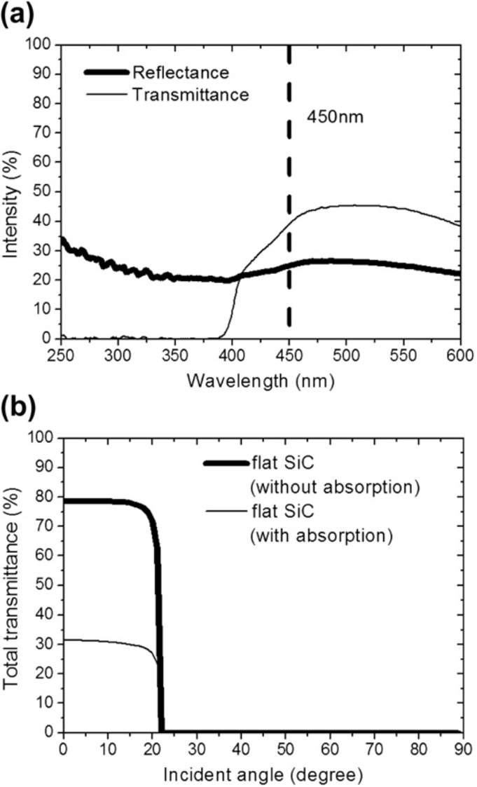
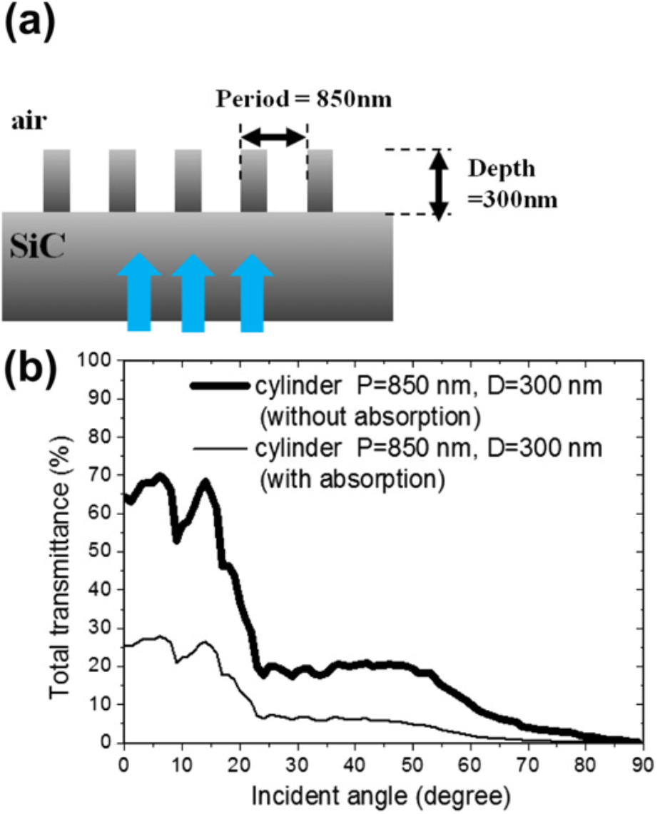
Simulations of light extraction and light propagation properties of light emitting diodes featuring silicon carbide substrates Although silicon carbide (SiC) possesses excellent material properties and is a good candidate to replace sapphire as the substrate material for high-power light emitting diodes (HP-LEDs), the light extraction behavior of SiC substrate-based gallium nitride (GaN) LEDs had not been reported in detail previously. In this study, we measured the optical properties of SiC substrates and determined their effects on SiC substrate-based LEDs. Because the optical constants of SiC are very different from those of sapphire substrates, the light propagating and light extracting behavior of SiC substrate-based LEDs differs dramatically from that of traditional sapphire substrate-based LEDs. Herein, we used rigorous coupled-wave analysis and finite-difference time domain methods to systematically analyze the light propagating behavior of flip-chip and conventional-type SiC substrate-based LEDs. Our measured and simulated data revealed that the absorption of the SiC substrate would seriously affect the light extraction efficiency of flip-chip SiC LEDs. For the conventional-type LEDs, on the other hand, because the refractive index of SiC is greater than that of GaN, light readily propagates through the GaN–SiC interface into the SiC substrate to form the SiC substrate guided mode, which cannot be extracted. Therefore, maximizing the first direct extraction light from conventional-type SiC LEDs would be the most effective approach toward increasing the light extraction efficiency. Accordingly, we analyzed some periodic structures that enhanced the light extraction efficiency of SiC substrate-based LEDs. |
(a) Measured reflectance and transmittance of a SiC plate having a thickness of 265 lm. (b) Simulated total transmittance, with and without considering the absorption of the SiC substrate.on.
|
|||
Copyright(c) 2008 Nano-optpelectronics Lab., Department of Material Science and Engineering, National Taiwan University No. 1, Sec. 4, Roosevelt Road, Taipei, 10617 Taiwan(R.O.C) Phone:+886-2-3366-3240 Fax:+886-2-2362-7651 |
|||||